it is a really simple, and fantastic way for mass production of your projects. Here’s a guide to get you from design to delivery.
Step 1: Designing with EasyEDA
EasyEDA is a website that works as a design tool, which is easy to use and also has direct integration with JLCPCB. Which makes them a great tool.
1. Sign Up and Start a Schematic: Create an account on EasyEDA and then open a new project. The schematic is the blueprint of the circuit, where you will add and connect components to each other.
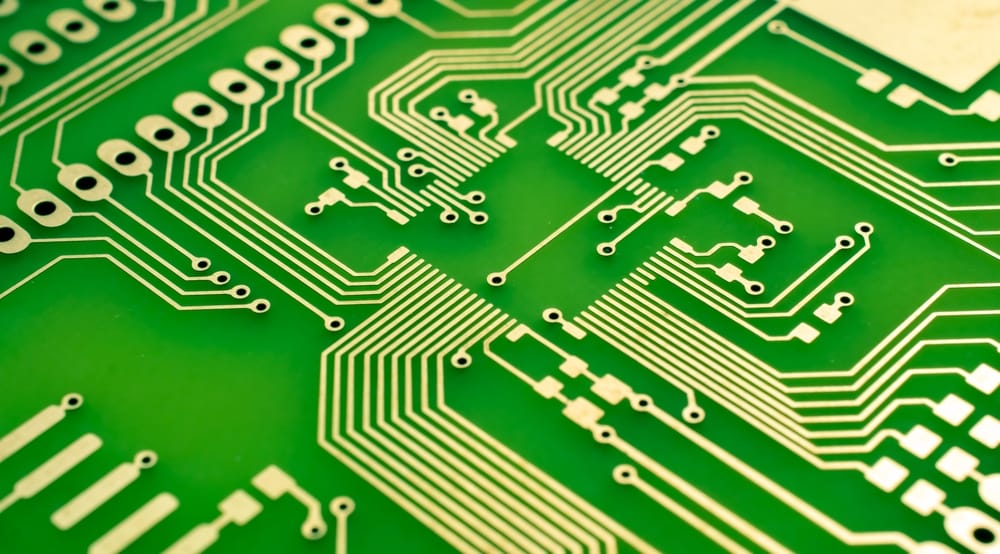
2. Arrange Components: Place parts on the board and connect them by drawing traces, like tiny copper roads for electrical signals. EasyEDA’s library has tons of components, including parts from LCSC (JLCPCB’s partner).
3. Check and Preview: Run a Design Rule Check (DRC) to ensure everything meets JLCPCB’s specs. Use the 3D preview to visualize your final board and spot any layout issues. In the end correct any problems that are evident.
Step 2: Export Gerber Files and BOM
Once your design is ready, you’ll need to export Gerber files. Gerber File is a format which JLCPCB employs to manufacture each layer of your board.
1. Generate Gerber Files: EasyEDA makes this easy-just go to Fabrication Output > Gerber Files.
2. Export BOM and CPL (if you want assembly): For JLCPCB to assemble the components, you’ll need a Bill of Materials (BOM) and a Component Placement List (CPL). EasyEDA can generate both easily.
Step 3: Upload to JLCPCB
1. Upload and Configure: Go to JLCPCB, upload your Gerber files, and check the preview. You can even customize settings like layers, board color, and thickness.
2. Optional Assembly: If you want JLCPCB to assemble components, upload your BOM and CPL files here, which were made by EasyEDA.
3. Select Shipping and Pay: Choose a shipping method based on your deadline or budget. Finally, complete the payment.
Step 4: Receive and Test Your PCB
After a short time period, your custom PCBs will arrive!
– Solder Components: In case you opted out of assembly, carefully solder the components yourself.
– Test Your Board: Before powering it up, use a multimeter to check for any shorts or open circuits. This quick step can save a lot of headaches of blasts and fire hazard.
Final Tips
– Double-Check Your Design: By reviewing connections and placements, errors can be avoided.
– Label Important Parts: Using silkscreen labels for key components makes assembly easier.
Enjoy your own PCB!


